|
Modification
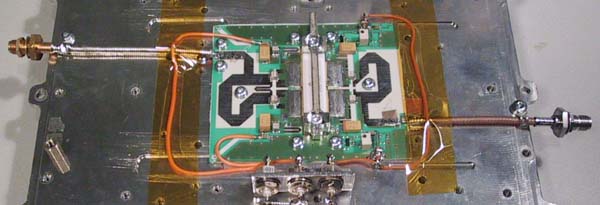
of a 100W 2,1GHz PA for 2,3GHz
Typical data on 2,3GHz after modification :
Gain: 9-10dB, Output power 100-120W
Active device is
Motorola MRF 21120
VDD 28V at 10A, bias +12V.
MRF21120 is a Gemini enhancement LDMOS transistor. It has a power
gain of typically 10 dB at 2,1GHz and about the same performance is
possible on 2,3GHz, but some adjustment is needed to squeeze the last
couple of tenth of dB out of the transistor. This PA was
originally made for 2,1GHz. It is a cut-out
from its original board. The VDD is +28V
and the bias input is +12V.
For full performance, a good size heat sink must be used. If the
temperature on the transistor wafer is allowed to rise above about +100
degrees Celsius, the LDMOS will reduce gain up to several
dB. If the heat sink is too warm, a fan must be used to cool the heat
sink.
Make sure that you have terminated both input and output into 50 Ohm
Then adjust each half of the Gemini to 0,8A idle current with no RF drive
applied. This assures linear operation of the PA.
It is very important that you provide a
perfect ground at your input and output terminals of the PCB. In this
example, a small piece of copper sheet is soldered on the heat sink side
of the PCB under the input and output terminals. The sheet is protruding
outside the PCB, thus providing a ground pad for the connecting coax
cable. Please note the nonexistent length of centre conductor from the
coax at the soldering point of the PCB.
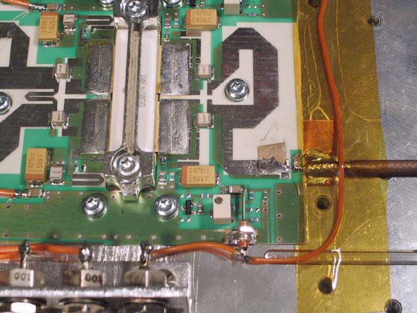
In the original, the input match is not
at optimum on 2,3GHz. This can easily be adjusted by increasing the pad
size close to the input on the PCB. The pad showed here may not
necessary be the same size on your board as it is an unique adjustment
for each PA. About one dB was found, bringing the
gain on 2,3GHz from 8,5 to 9,5 dB on this sample PA.
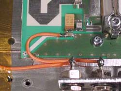
To provide a PTT line, a relay or similar can
remove the +12V bias. The idle current will then go to zero without need
to remove the VDD when PTT is in RX.
 |
When you connect VDD to the PCB,
take care not to short it to ground as one end of the trace is
feed to the heat sink side of the PCB. In the PA used here, I have
cut of the copper trace close to the decoupling capacitor and
soldered the VDD cable close to the capacitor
(the orange cable). |
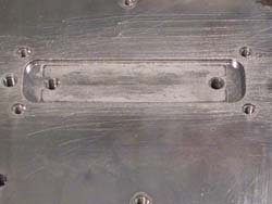 |
Make
sure that the transistor has a slot 1,3mm deep to allow the PCB to be
absolutely flush with the heat sink. All provided screws holes must be used
if you want the available power into your output coax. All
microwave design rules apply!! A note of caution, to not drill out
the through plated holes in the PCB, to make room for bigger screws
than the original size of 2,5mm. |
For a 400W PA see the OH3LWP solution
http://oh3tr.ele.tut.fi/~ftp/pa/13cm_400W_LDMOS_PA/
|